SEMI (International Semiconductor Industry Association) and TechSearch International jointly released the Global Semiconductor Packaging Materials Outlook, predicting that the global semiconductor packaging materials market will follow the growth pace of the chip industry. The market revenue will rise from 17.6 billion dollars in 2019 to 20.8 billion dollars in 2024, with a compound annual growth rate (CAGR) of 3.4%.
The growth of this wave of semiconductor industry is driven by various new technologies, including big data, high-performance computing (HPC), artificial intelligence (AI), edge computing, front-end access memory, the expansion of 5G infrastructure, the adoption of 5G smart phones, the growth of electric vehicle usage, and the enhancement of vehicle safety.
Packaging is a core part of the semiconductor industry, and its main purpose is to protect chips. The semiconductor packaging test is at the later stage of the wafer manufacturing process. After the chip is manufactured, the wafer is packaged and tested. The wafer that passes the test is processed according to the needs and functions to obtain the chip. It belongs to the later stage of the whole IC industry chain. The four main purposes of packaging are to protect the chip, support the chip and its shape, connect the chip's electrode with the external circuit, and enhance the thermal conductivity, The specification standardization is realized and it is convenient to connect the I/O port of the chip to the printed circuit board (PCB), glass substrate and other materials at the component level (system level) to realize circuit connection and ensure the normal operation of the circuit.
| Packaging process determines the performance of semiconductor
Encapsulation must meet certain requirements for mechanical, thermal and chemical characteristics, or it will directly affect the packaging effect and the reliability of the entire device. Flow and adhesion are two main physical properties that must be optimized for any encapsulation material. The coefficient of thermal expansion (CTE) within a specific temperature range and the glass transition temperature (Tg) beyond the reliability test range (- 65 ℃ to 150 ℃) are critical to the firmness of the package.
Chip packaging process flow includes incoming material inspection, film pasting, grinding, patch, scribing, scribing detection, loading, bonding, plastic packaging, marking, rib cutting and bending, quality inspection, and finally product shipment. In this process, packaging materials such as packaging substrate, lead frame, bonding wire, packaging materials, ceramic substrate, bonding materials are needed.
| Packaging substrate: the largest material in packaging field
In 2021, the overall scale of the global IC packaging substrate industry will reach 14.198 billion US dollars, with a year-on-year growth of 39.4%, which has surpassed the flexible board and become the fastest growing fine molecule industry in the printed circuit board industry. In 2021, the market size of China's IC packaging substrate (including foreign manufacturers' factories in China) will be 2.317 billion US dollars, with a year-on-year growth of 56.4%, maintaining a rapid growth trend.
At present, the global packaging substrate manufacturers are mainly distributed in Japan, South Korea and Taiwan, China, China. The market pattern is relatively scattered, and the localization rate is low, less than 5%.
| Lead frame: IC and power device carrier, with high localization rate
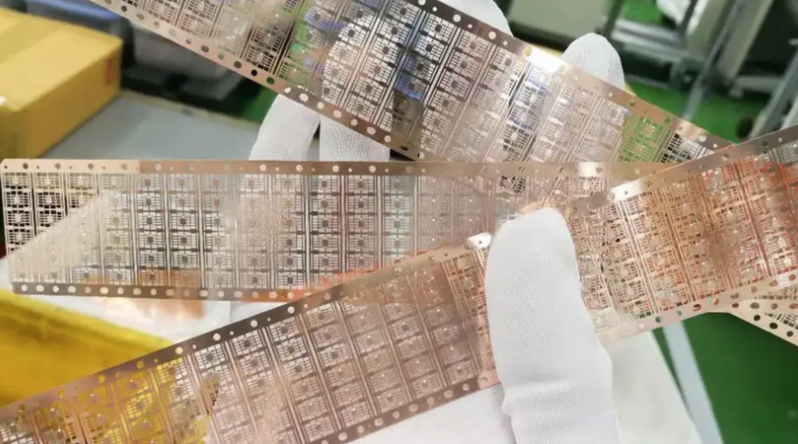
The lead frame is a carrier of integrated circuit chip. With the help of bonding wire, the leading out end (bonding point) of the internal circuit of the chip is electrically connected with the external lead through the internal lead to form a key structural part of the electrical circuit. Its main functions include chip stabilization, signal transmission, heat transmission, etc.
According to SEMI data, the size of the global lead frame market has remained stable all the year round, reaching US $3.195 billion in 2020, with a year-on-year growth of 3.5%. In terms of market pattern, after Taiwan, China manufacturers acquired some Japanese manufacturers, Japanese and Taiwan, China manufacturers now dominate the market.
According to the data of Microenterprise Consulting, in 2019, the market size of China's domestic manufacturers' lead frame was 3.42 billion yuan, accounting for 40% of China's lead frame market, and the remaining 60% was still supplied by foreign manufacturers. There are many Chinese manufacturers, but most of them mainly produce stamping lead frames, including Hualong Electronics, Yonghong Technology
Fengjiang Microelectronics, Huajing Lida, Jingheng Precision, Jinwan Electronics, Sanxin Electronics, Dongtian Electronics, etc. In terms of more high-end etching lead frame, only a few manufacturers such as Kangqiang Electronics, Huayang Technology, New Henghui, Leader Semiconductor, Core Hengchuang Semiconductor can produce
| Bonding wire: bridge for electrical connection between IC and lead frame
Bonding wire is a fine metal wire with a diameter of tens of microns to tens of microns, which is used to realize the electrical connection between the circuit input and output connection points in the chip and the internal contacts of the lead frame. The upstream raw materials are mainly gold, silver, copper, aluminum and other metals, the middle reaches are produced by bonding wire, and the downstream applications are integrated circuits and discrete devices.
According to CEPEM data, the market size of bonding wire in 2019 is about US $2 billion. In terms of product segmentation, bonding alloy wire accounts for 32%, palladium plated copper wire accounts for 29%, pure copper wire accounts for 25%, bonding silver wire accounts for 12%, and aluminum wire accounts for 2%.
The bonding wire market in China is still mainly occupied by German, Korean and Japanese manufacturers, and the products of local manufacturers are relatively single or low-end. According to CEPEM data, German Heraeus accounts for 21%, Korean MKE accounts for 20%, and Japan Railway and Tanaka account for 13% and 10% respectively. The Chinese manufacturer Yinuo Electronics is the largest manufacturer with local capacity, accounting for 11%, while Wansheng Alloy, Dabo Nonferrous and Mingfeng Technology account for 6%, 5% and 2% respectively. In addition, Kangqiang Electronics also has a layout in bond alloy wire and bond copper wire.
| Ceramic substrate: emerging heat dissipation materials
With the technical progress of power electronic products, the problem of heat dissipation has become a bottleneck that restricts their development towards high-power and lightweight. As a new heat dissipation material, ceramic substrate has excellent electrical insulation performance, high thermal conductivity, and both thermal conductivity and insulation are better than metal substrate. It is more suitable for packaging of power electronic products. It has become the basic material for high-power power electronic circuit structure technology and interconnection technology, and is widely used in industrial electronic fields such as LED, automotive electronics, aerospace and military electronic components, laser
Common ceramic substrate materials for electronic packaging include aluminum oxide (Al2O3), aluminum nitride (AlN), silicon nitride (Si3N4), beryllium oxide (BeO), boron nitride (BN), etc. Al2O3 and AlN have good comprehensive performance, occupying the mainstream in low-end and high-end ceramic substrate markets respectively. Si3N4 substrate plays an important role in the packaging field of high power, large temperature change power electronic devices (such as IGBT) due to its outstanding comprehensive performance. Although the price of AlN is about 4 times that of Al2O3, due to its high thermal conductivity and better heat dissipation, AlN is the most commonly used substrate, followed by Al2O3.
On the whole, the key to the sustainable growth of the above technology applications lies in the front-end packaging technology. The largest laminated substrate of packaging materials will have a compound annual growth rate of more than 5% due to the demand for system level packaging (SIP) and high-performance devices; The report predicts that the 9% compound annual growth rate of dielectric in wafer level packaging (WLP) is the fastest. Although various new technologies to improve performance are being developed, the development trend of smaller and thinner packaging will become a resistance to the growth of lead frames, die attachs and sealants.


