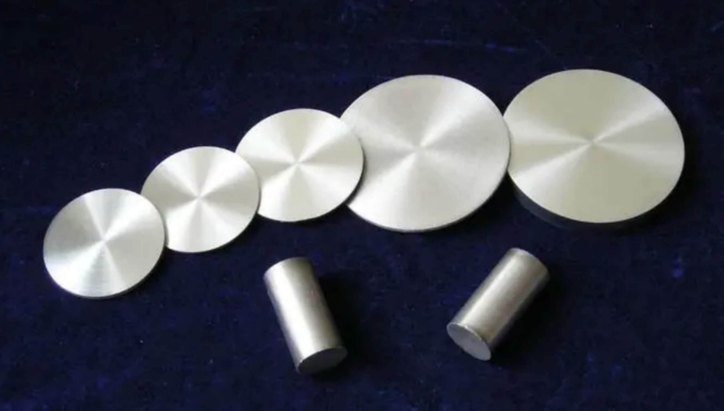
In the semiconductor industry chain, there is a low-key but crucial material, which is the target. The target we are talking about here is not the target for archery, but a high-speed nuclear particle. Different films can be obtained through different targets. Although the target is not as conspicuous as silicon chip or photoresist, its effect cannot be underestimated. In 2025, the global market size will reach 33.3 billion dollars. At present, the four giants of Japan and the United States in the world occupy 80% of the target material market, and there is a strong demand for domestic substitutes.
| Small target, big effect
Many people may be unfamiliar with the target, but it has long been hidden in your life, such as our inseparable mobile phones. The chip is the soul of the mobile phone, so the target we are talking about here is the soul of the chip. There are many dense metal wires on the chip. These metal wires are not welded manually, but must be high-purity metal targets, which are completed by sputtering. Sputtering is the main technology for preparing thin film materials. It uses ions generated by ion sources to accelerate their aggregation in vacuum to form high-speed ion beams, bombard solid surfaces, and exchange kinetic energy between ions and solid surface atoms to make atoms on the solid surface leave the solid and deposit on the substrate surface. The bombarded solid is the raw material for depositing thin films by sputtering, which is called sputtering target.
For example, the Apple A16 processor, a chip the size of a fingernail, is densely covered with tens of thousands of meters or more of metal wires. Of course, these densely covered circuits cannot be manually welded. High purity metal targets must be sputtered, which can be approximately understood as a 3D printing process. However, this process is more microscopic and accurate, and the target is the raw material for sputtering coating.
Target materials are located in the middle reaches of the industrial chain. According to different downstream applications, there are many kinds of target materials, which can be divided into alloy target, ceramic target and metal target according to materials, and can be used in panel display, semiconductor, photovoltaic and other fields. Among them, semiconductor production has higher requirements for the purity of target materials.
| The localization rate of target materials in China is less than 10%
In 2020, the global target market size will be about 18.8 billion US dollars, and the target market size in China will also reach 4.6 billion US dollars, which is expected to achieve long-term stable high-speed growth in the next few years. Among them, the demand for photovoltaic target materials comes from the technological transformation of HJT cells and thin film cells, the demand in the semiconductor field comes from the transfer of wafer production capacity to China, and the display panel is based on the trend of expanding panel size and the continuous expansion of domestic production capacity.
The target material is a typical small and beautiful key material. Take the semiconductor as an example. Although the cost of the target material accounts for only 3% of the previous cost of the semiconductor, it plays a vital role. As mentioned earlier, the role of sputtering target is to act as a metal wire to transmit information on the chip, with a diameter of only nanometers, connecting hundreds of millions of micro transistors inside the chip.
However, the localization rate of such a key raw material in China is less than 10%.
At present, there are mainly four enterprises in the global sputtering target market, namely JX Nippon Metals, Honeywell, Dongcao and Praxair, with market shares of 30%, 20%, 20% and 10% respectively, which together monopolize 80% of the global market share. Among them, the American and Japanese multinational groups have complete industrial chains, including metal purification, target manufacturing, sputtering coating and terminal application. They have the capacity of large-scale production. After mastering advanced technologies, they implement monopoly and blockade, leading the technological innovation and industrial development, and have obvious advantages in the field of high-end semiconductor sputtering targets.
In the target industry chain, China mainly focuses on the low-end areas, target manufacturing and target coating, with relatively low technical barriers. Most domestic target enterprises focus on this area.
Technical barriers make it not so easy to replace domestic products
The target has a very high technical barrier, and the purity is the most important technical indicator. Generally, the purity of semiconductor targets is required to reach 99.9995% (5N5) or even 99.9999% (6N), and some even reach 9N or more. It is also easy to understand that, after all, silicon chips require such high purity that the requirements for auxiliary materials cannot be lowered. For example, if you want to lose weight by eating salad, you can certainly not use substances with high calories such as lard when dipping in sauce. The requirements for panel targets and photovoltaic targets are slightly lower, but the purity is also above 4N. This process is accompanied by a "breathtaking leap". The price of high-purity targets is far beyond that of ordinary metals. For example, the price of high-purity aluminum is up to 120000 yuan/ton, nearly 10 times more expensive than ordinary aluminum ingots.
In addition, the barrier of target materials is also reflected in the certification time. It takes a long time from new product development to mass supply, generally 2-3 years. At the same time, subsequent new entrants need to significantly exceed the original suppliers in terms of technical level, product quality, follow-up services and supply prices, so as to have the possibility of obtaining business cooperation opportunities.
Although the target industry chain is not long, it is also quite uneven. The highest profit rate is the metal purification link, and the preparation of high-purity metal raw materials is the premise of subsequent production. For a long time, domestic manufacturers have mainly obtained the supply of high-purity metals through imports from abroad. High purity metal manufacturers in the United States, Japan and other countries have strong bargaining power for downstream based on advanced purification technology, which has increased the production cost of target materials. However, most of the terminal application manufacturers are large wafer factories and panel factories with strong bargaining power. The technical barriers of target manufacturing and target coating in the middle are relatively low. Unfortunately, most domestic target enterprises are concentrated in this field.
| Huge market demand becomes the breakthrough of reversal
At present, domestic ITO target materials are mainly supplied to the low-end market, with a market share of about 30%. There is a large demand for import substitution. As a key raw material for semiconductors, display panels, photovoltaic cells, etc., it is estimated that the global market size will reach 33.3 billion dollars in 2025. However, at present, four Japanese and American giants occupy 80% of the target market, and there is a strong demand for domestic substitutes.
In recent years, with the transfer of downstream industries to China and the breakthrough of domestic target material process and raw material purification process, domestic aluminum, copper, molybdenum, ITO and other varieties have made targeted breakthroughs and entered the downstream mainstream customer supply system. From the downstream perspective, we believe that the semiconductor target market, display panel target market and photovoltaic panel target market will have a large growth space in the future. It is estimated that the scale of China's semiconductor target market will reach US $670 million in 2025, and the CAGR will be 9.2% in 21-25. The market scale of display panel target is about US $5 billion, with CAGR of 18.9% in 21-25 years. The market size of photovoltaic target materials will be close to USD 3.8 billion, with CAGR of 56.1% in 21-25 years.


