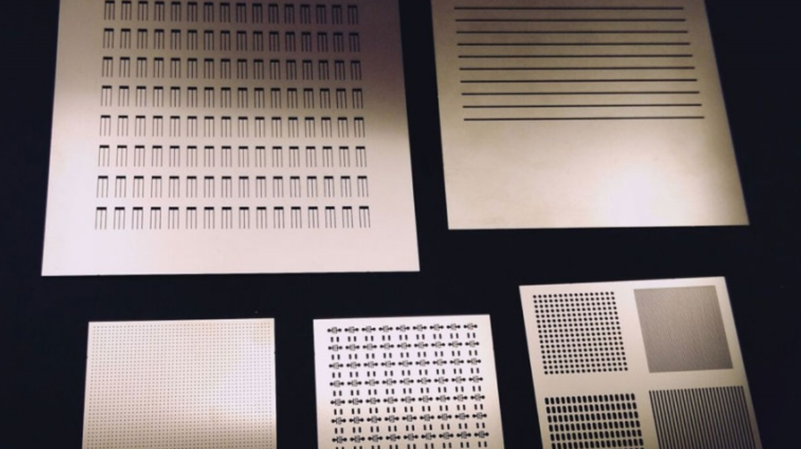
Silicon Semiconductor industry about 37 percent of the List of semiconductor materials's cost, followed by mask and semiconductor gas, which account for about 13 percent, according to the International Association of Electrical and Mechanical Engineers. Therefore, mask is a key material in semiconductor chip manufacturing.
At present, China is the world's largest semiconductor market demand, the scale of the integrated circuit market continues to rise, the future growth space is broad, the mask version market demand is considerable.
| What's a mask?
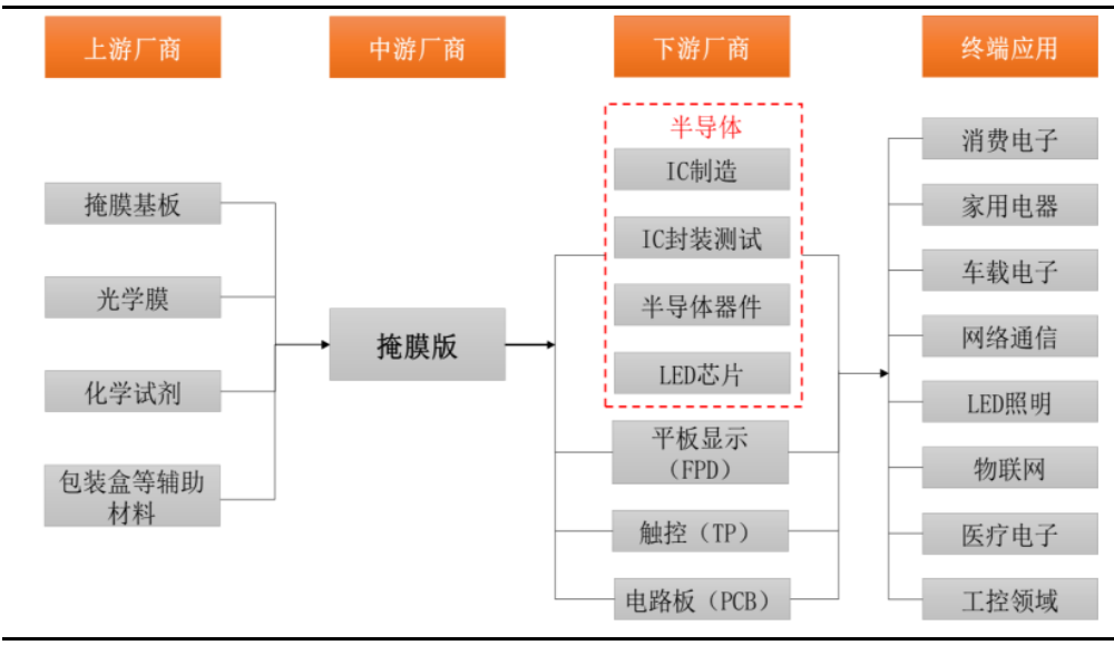
Masking plate is an ideal photosensitive blank plate for fabricating micro-mask patterns, which can be obtained by photolithography process. In the industry chain, the mask plate's main raw materials include mask substrate, optical film, chemical reagents and packaging and other auxiliary materials, it is mainly used in the manufacturing process of flat panel display, semiconductor, touch control and circuit board. It is one of the essential key materials.
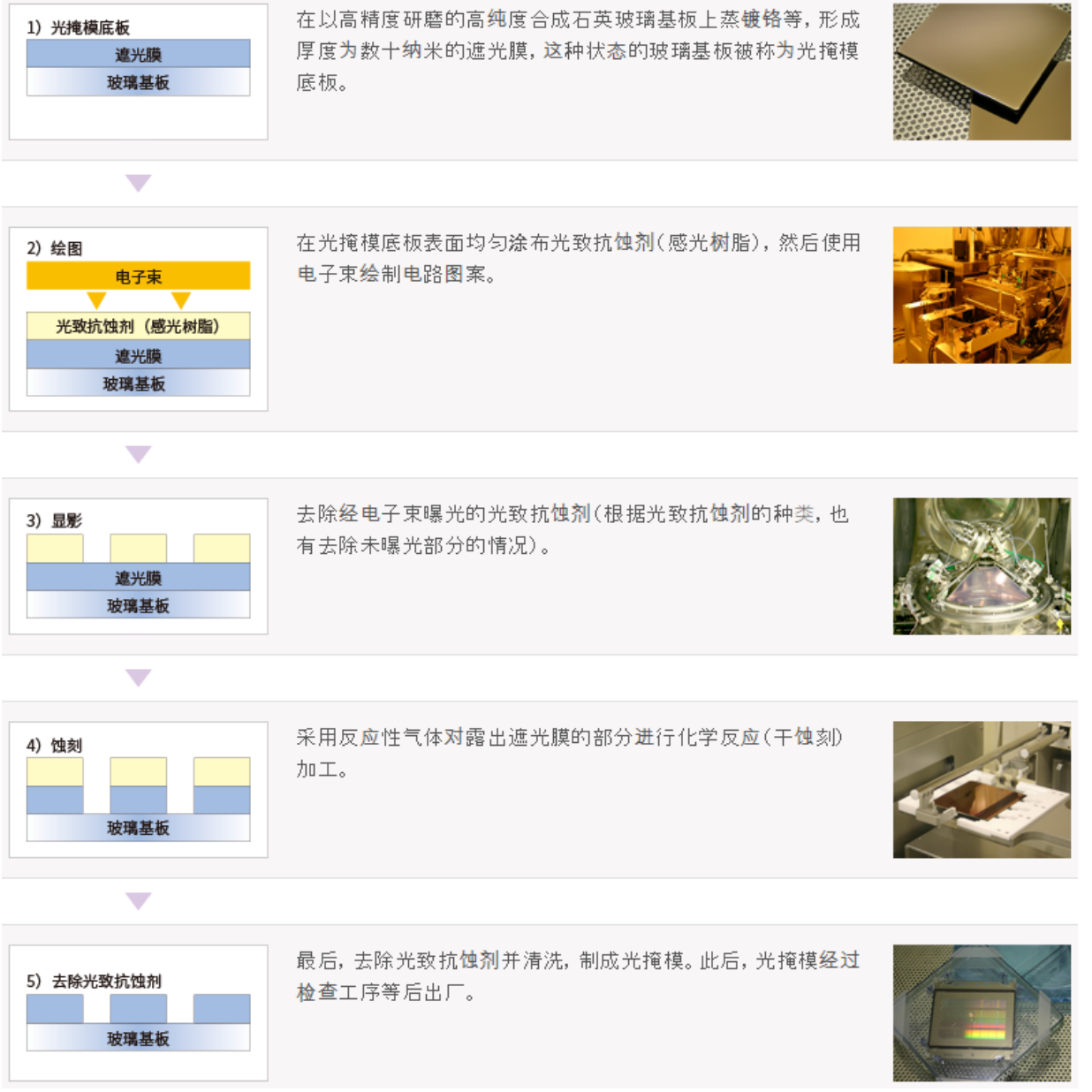
A basic overview of the mask
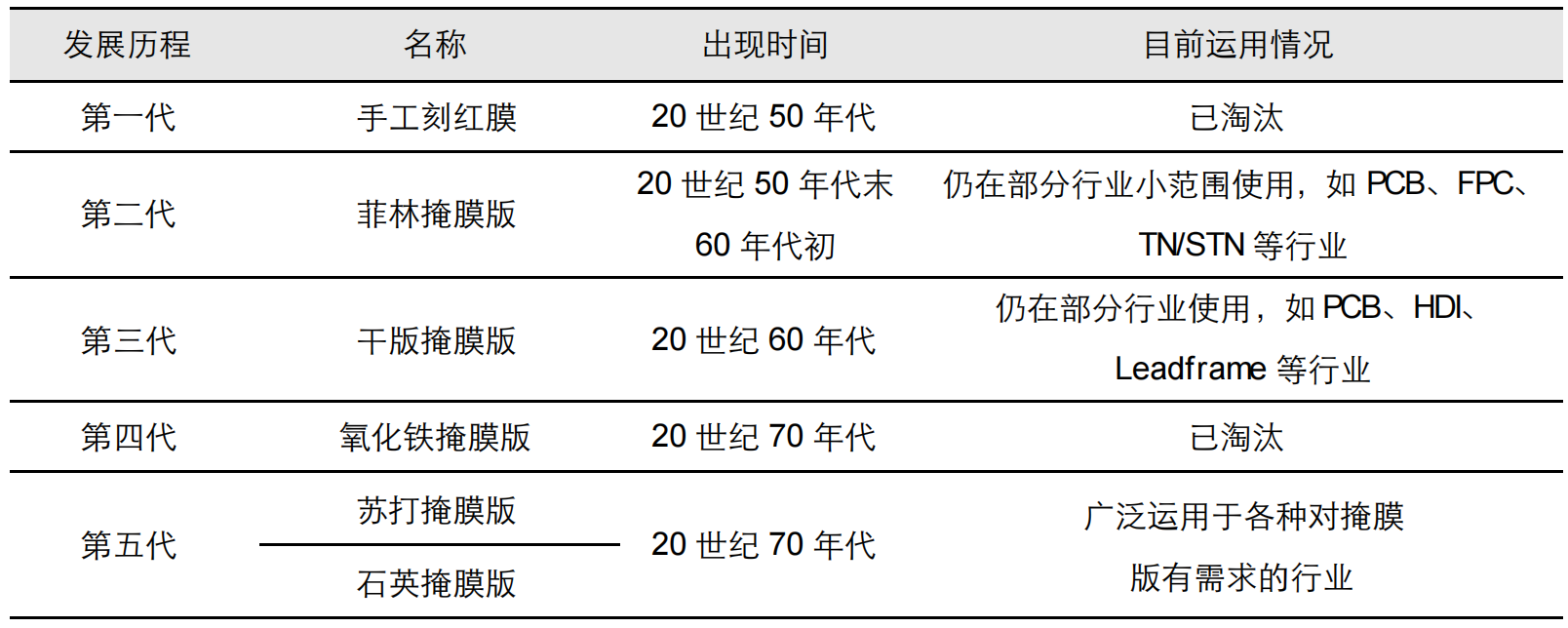
Since its inception, the mask has been developed into the fifth generation of products, which have undergone hand-carved red film, photographic film version, dry version, iron oxide, Soda and quartz version, some of the first four generations of products have been eliminated, some are still used in some small industry, the fifth generation of soda and quartz mask since the 1970s, the most widely used.
According to the use of points, the mask can be divided into chrome (chrome) , dry, liquid relief and film. Among them, chrome plate is widely used in IC, flat panel display, PCB and other industries because of its high precision and good durability Dry Plate, liquid relief and film are mainly used in low-precision LCD industry, PCB and IC board and other industries. In terms of downstream applications, IC and flat panel displays accounted for the largest share, with semiconductors accounting for 60% , LCD for 23% , OLED for 5% and PCB for 2% .
The size of the mask market
The global market for Photomask is growing year by year. In 2017, the global semiconductor chip mask market was $3.7 bn, up 13 per cent year-on-year, and in 2019 it was about $4.3 bn, according to Semi.
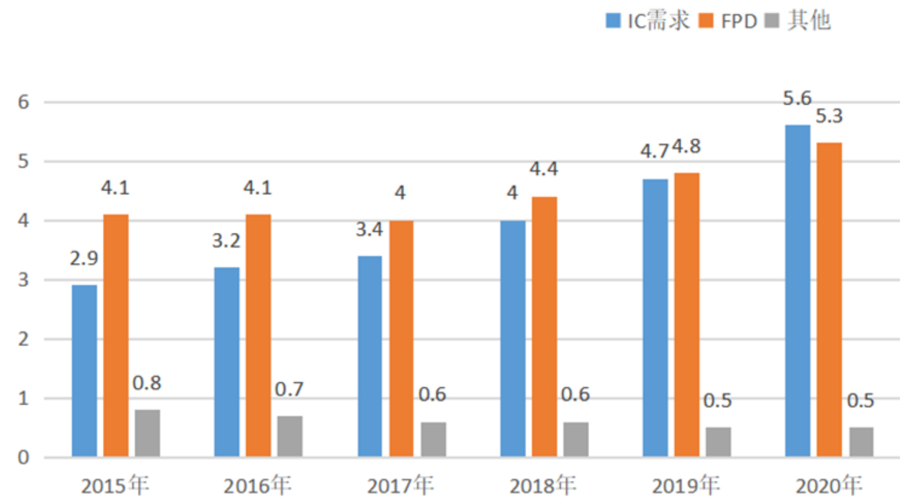
In terms of domestic demand, China's semiconductor photomask market reached US $144 million in 2019. From the specific demand for glass substrates, the demand of IC photomask glass substrate increased from 29,000 square meters in 2015 to 56,000 square meters in 2020, catching up with the demand of FPD (flat panel display) for the first time.
According to the data, China's integrated circuit market will reach 1139.7 billion yuan in 2022, and the semiconductor mask market will be 5.3 billion yuan in 2020, and is expected to reach 9.4 billion yuan in 2025.
Mask competition pattern
In the semiconductor field, there are two types of manufacturers: wafer/IDM factories and independent third-party manufacturers, including Intel, Samsung, TSMC, SMIC International, China Resources Micro (Diswell) and so have their own mask business. As the mask involves Foundry technical secrets, Foundry factory advanced process (45 nm below) most of the mask used by their own professional factory production, however, Foundry preferred to purchase from independent third-party mask manufacturers to reduce the cost of the more standardized masks used in more mature processes, such as 45NM and above.
Among the manufacturers, the proportion of wafer/IDM factories has increased steadily. In 2008, the proportion was only 39% . In 2018, it reached 64% . In 2019, it reached 65% . Independent third-party mask manufacturers accounted for 35% .
The world's independent third-party mask manufacturers are mainly concentrated in Japan and the United States, including Japan Toppan (letterpress printing) , Japan DNP (Big Japan Printing) , the United States Photronics (fornix) , Japan Hoya (Hoya) , Japan Ske (SK Electronics) , South Korea LG-IT (LGInnotek, LG Group subsidiary) , etc. , there are also Chinese manufacturers such as China Taiwan Optical Mask, Joe Luwi Optronics and Qingyi Optronics.

Domestic mask development pain point
Because the mask is an important link between design and manufacturing, wafer manufacturers have their own professional factory to produce their own needs mask. Such as Intel, Samsung, such as the international big factory, will mask manufacturing process firmly in hand, set up their own mask factory. Therefore, advanced mask technology is also mastered in the advanced wafer manufacturing process in the hands of the wafer factory
2, semiconductor mask high investment, small-scale, high technical precision, and product zero defects, and so on, many companies are afraid of no return, domestic scale, market-based mask version of the enterprise few. Domestic professional production of mask version and larger enterprises are: Joe Luwi optoelectronics, qingyi optoelectronics, smic, but Joe Luwi optoelectronics, qingyi optoelectronics is mainly used to do the screen photomask version.
3.2 the main technical difficulties are as follows: first, the light transmittance of the material, which is 100% opaque to the mask and 100% transparent to the substrate, and second, the purification technology, which needs to purify the quartz to the electronic level (the minimum purity requirement is 99.9999%) . Because our country technology is not mature before, can only be quartz stone shipped abroad, after grinding, refining, purification and a series of high-difficulty process, processing into quartz ingots, and then buy back at a high price. The import and export price of quartz stone is very different. The export price of quartz stone is US $400/ton, and the import price of quartz ingot is US $10000/ton.
Mask trends
Generally speaking, Chinese mask manufacturers' products are in the middle and low end as a whole, the Chinese mainland capabilities of independent third-party semiconductor mask manufacturers are focused on masks for wafer fabrication above 100 nm nodes and on IC encapsulationic device masks, with the international leading enterprises have a more obvious gap.
According to the mode of operation, there are three types: the first type is scientific research institute, including Institute of Semiconductors, Institute of Microelectronics, Institute of Electronics, 13/55/47, etc. . The second type is independent mask manufacturers, the third category is the wafer factory to support their own production mask version, mainly smic, China Resources Micro (dismicro) and so on.
Trends:
1. Refine
2. Go Big
3. Mask manufacturers extend to the upstream industry chain: the main raw material of mask is mask substrate, in order to reduce the cost of raw materials, control the quality of end products, mask manufacturers have begun to extend their production chain upstream. Some enterprises, such as Hoya and LG-IT, already have the production capacity of grinding/polishing, chrome plating, photoresist coating, etc. , joe Luwi and Qingyi made breakthroughs in photoresist coating. The future mask version industry has a certain strength of enterprises, will gradually expand to the upstream industrial chain.


