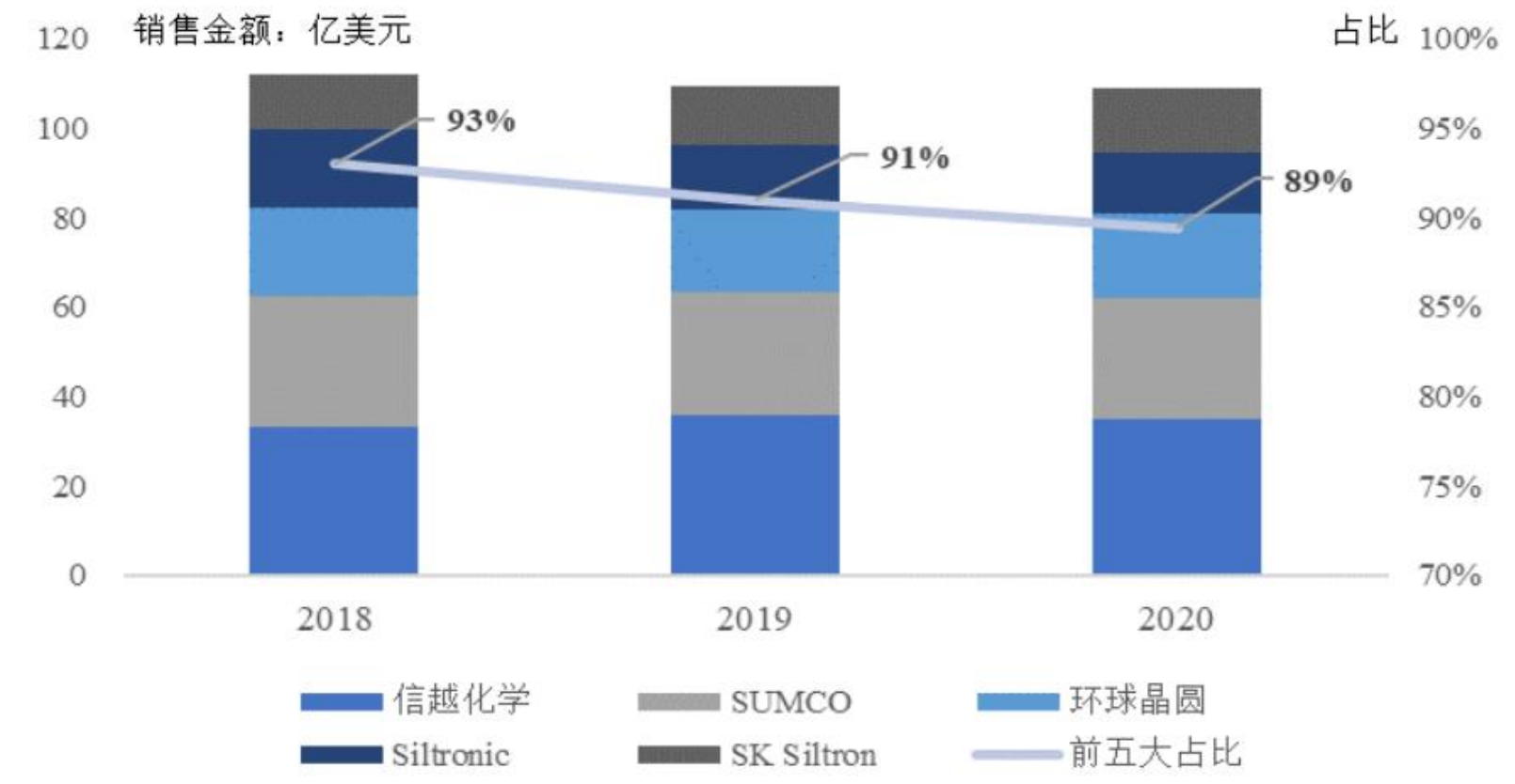
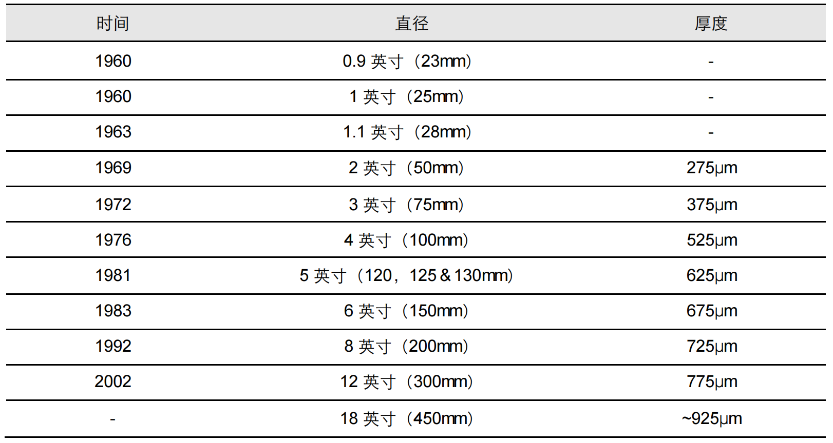
Silicon wafers are the starting point for chips, 2021 the $14bn global market for semiconductor silicon wafers, a highly concentrated industry with a CR5 market share of nearly 90 per cent. Silicon is the most widely used List of semiconductor materials, making up more than 90% of semiconductor products. With the rapid penetration of 5G, new energy and AIoT, the 2021 semiconductor industry has entered a super-boom cycle, and demand for silicon wafers continues to be strong. The global area of semiconductor silicon wafers shipped reached 14.2 billion square inches, up 14% year-on-year, the market is $14bn. The periodic fluctuation of semiconductor industry leads to the periodic fluctuation of demand for silicon wafers. The merger and integration of silicon wafers industry is continuous, and the competition pattern is highly concentrated. The market share of the top 5 manufacturers is close to 90% . New silicon wafer capacity needs to be released to the 2024, short-term supply and demand is expected to remain tight, long-term LTA to help price stability. Silicon wafer expansion cycle in more than two years, the world's 12-inch silicon wafer by 2020 mainly rely on the existing plant capacity expansion, new plant capacity release will peak after the 2024, 2022 and 202312-inch silicon wafers worldwide will remain in short supply. This capacity expansion, downstream wafer factories and wafer manufacturers actively binding, through long-term agreements to ensure supply chain stability. Silicon: the foundation of the Semiconductor industry, the starting point of the chip Semiconductor silicon wafer is the key material to produce semiconductor products such as integrated circuits, discrete devices, sensors and so on. Among many semiconductor raw materials, silicon has obvious advantages, such as high melting point and wide band gap, which can be widely used in high temperature and high voltage devices. In addition, silicon has a natural high-quality insulating oxide layer that reduces the deposition of insulators during wafer fabrication, thereby reducing production steps and reducing production costs. Silicon is abundant in nature, accounting for about 27 percent of the Earth's crust, and the cost of silicon materials is significantly lower than other types of List of semiconductor materials. Because of its technology and cost advantages, silicon wafers are now the largest and most widely used List of semiconductor materials, accounting for more than 90% of all products and a fundamental part of the Semiconductor industry chain. According to the classification of manufacturing process, semiconductor silicon wafers can be divided into polishing wafers, epitaxy wafers and high-end silicon-based materials represented by SOI wafers. Industry cycle fluctuation, oligopoly pattern Semiconductor silicon wafers are subject to downstream chip boom, with a certain periodicity, the cycle is usually 3-4 years. In 2020, with the“Epidemic economy” and the rapid penetration of 5G, new energy and AIoT, the demand for chips is increasing, the demand for silicon wafers is also increasing, semiconductor silicon wafers in the boom cycle, the 2021 shipped 14.2 bn sq ft of silicon wafers, up 14 per cent year-on-year. Competition pattern: the market is highly concentrated The global silicon chip market is highly concentrated, the top five manufacturers account for about 89% of the market share, leading Japanese silicon chip companies. Japanese companies have been leading the way in semiconductor silicon wafers, with Shin-Etsu and SUMCO taking a combined market share of more than 50 per cent. In December 2016, global wafers paid $683m for SunEdison Semiconductor of the US, then the world's fourth-largest Semiconductor manufacturer. Following the acquisition, global wafer became the largest supplier of semiconductor silicon wafers in Taiwan, China and the third largest in the world. SKSILTRON and Hynix are both part of SK Group. With the rapid development of the storage market, the share of SKSILTRON continues to increase. Domestic silicon wafer company echelon effect is obvious, leading company develops rapidly. Shanghai silicon industry, Léon Micro and other large-scale silicon wafer technology accumulation and production capacity advantage, in the revenue end gradually with other silicon wafer companies open gap to achieve faster growth. What overseas companies have in common: 1 product variety is relatively complete → easier to attract customers: overseas leading product variety is more rich, easy for customers to choose products, more easy to attract customers 2 high yield → increasing profitability: the purity and yield of silicon wafers require long-term trial and error and continuous process optimization. High technology determines the high purity and high yield of silicon wafers. At the same time, yield can share the cost of manufacturing, so high process technology also brings better profitability for the company 3 m & a integration → expand market share: overseas leading companies all choose to expand market share through M & A. The 7.3-magnitude earthquake in Japan has severely affected the supply of 12-inch silicon wafers in Shinetsu. The price of silicon wafers will continue to rise as a result of the“Silicon Shortage + five major companies begin to release production capacity in more than 23 years and 24 years”. The three characteristics of the industry Feature 1: large input line, high depreciation costs. According to estimates by silicon research, it would cost 385 million yuan to produce 100,0008-inch wafers a month, while the investment of 100,00012-inch wafers a month is four times the size of 8-inch wafers, or about 1.6 billion yuan. The main reason for this is that the 12-inch wafer is used in the narrower linewidth process, which requires finer and more stringent specifications for single-crystal microdefects, wafer flatness, surface particulate matter, and surface contamination. Compared with 8-inch, 12-inch silicon wafer production process is more complex, also added such as rough grinding knife, fine grinding knife, double-sided polishing machine and other special equipment. In addition, in the processing mode, 12-inch processing equipment mostly uses monolithic processing mode, while 8-inch processing equipment mostly uses batch processing mode, so the same capacity needs to invest a greater number of equipment. From the current mainstream silicon wafer manufacturers, depreciation and amortization of the proportion of revenue in the 10% -15% , depreciation costs higher. Feature Two: Gross Margin Volatility. Gross margins fluctuate depending on the price and Capacity utilization at which the chip is sold. The global average price of semiconductor silicon wafers was in a sustained downward trend from 2011 to 2016, reaching a low of $0.67 per square inch in 2016. As wafer capacity continues to expand and downstream demand picks up, particularly for storage products, the average price of silicon wafers has risen by 10 per cent in 2017 and 20 per cent in 2018. Feature 3: the proportion of long-term supply agreement (LTA) continues to increase. The continued increase in LTA's share has helped to reduce the volatility of silicon wafer prices. During the market downturn in 2019, the performance of silicon wafer companies with a higher LTA share (such as Globawafers, Sumco, etc.) has been relatively less volatile, changxie accounted for lower companies, such as Taiwan Branch, whose revenue fell 28.9 percent in 2019. “Big size” is the trend for silicon wafers Silicon wafers can be divided into 50mm (2 inches) , 75mm (3 inches) , 100mm (4 inches) , 150mm (6 inches) , 200mm (8 inches) and 300mm (12 inches) depending on their size. At present, 8-inch and 12-inch silicon wafers are the most popular products on the market. The 8-inch silicon wafer is mainly used in 90nm-0.25 μm process, and is widely used in the fields of sensing, security and power devices of electric vehicles, analog IC, fingerprint identification and display drive, etc. . 12-inch wafers are used in processes below 90 nm for logic chips, memory, and autopilot applications. The larger the wafer size, the more chips there are on a single wafer, thus increasing production efficiency and reducing production costs. 300mm silicon is 2.25 times the area of 200mm silicon, according to silicon crystal Structure and Growth data, take 1.5 cm × 1.5 cm silicon as an example, 300mm silicon chip 232,200mm silicon chip 88, the number of 300mm silicon chips is 2.64 times that of 200mm silicon chips. According to the data, the 2021 of large silicon wafers, represented by G12 and M10, rose rapidly from 4.5% in 2020 to 45% in 2010. According to CPIA, the combined market share of large-size silicon wafers is expected to exceed 85 per cent by 2023, even though nominal capacity may be under pressure, however, M10, G12 and other large-scale silicon wafer supply or still remain phased tight state. 210/M12/G12 large silicon wafer photoelectric conversion efficiency and production efficiency have obvious advantages, large-scale silicon wafer cost reduction and efficiency increase effect is obvious. It is widely expected that the permeability of large-size silicon wafers will accelerate in the next three years. The future of silicon 1) short-term: large-scale capacity is still in short supply. At the end of the 2021, nominal wafer capacity is expected to be above 350GW, which looks like a glut over demand -- about 210GW of new capacity will be installed in 2022, corresponding to 250GW of wafer demand -- but actual large-scale capacity is still in short supply. According to CPIA, large size is expected to account for 90% of the market by 2022. 2) medium-and long-term: the price of silicon wafers is a historical trend, the photovoltaic industry gradually out of subsidies, become affordable access to the Internet, then demand will really explode. Core concern: head manufacturers have better cost control capabilities, as well as better financing capabilities, in the industry during the downturn, the ability to resist risk. High-end 12-inch product localization rate is very low, leading edge prominent, the proposed Pre-IPO round and other late projects.


