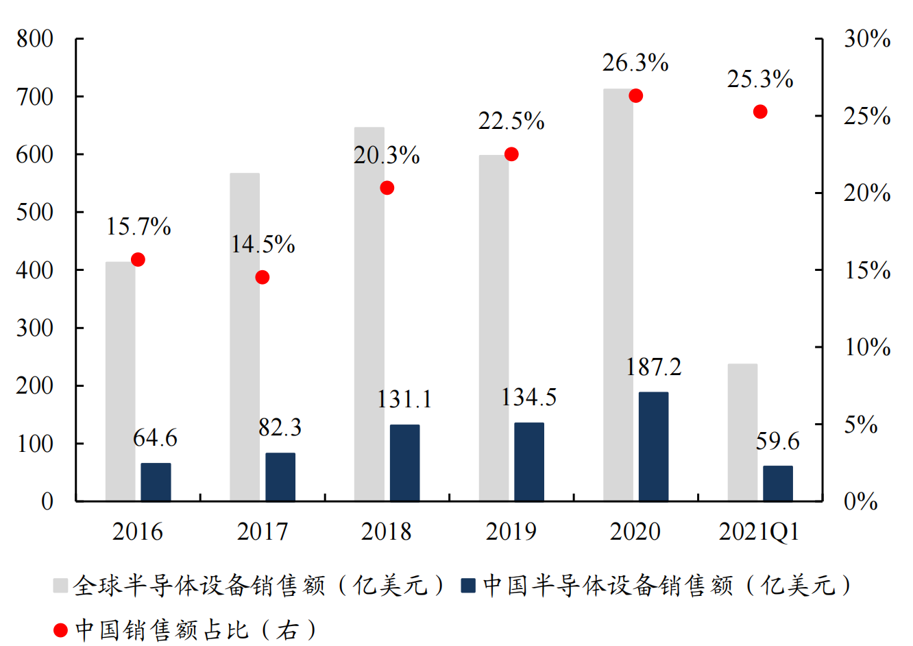
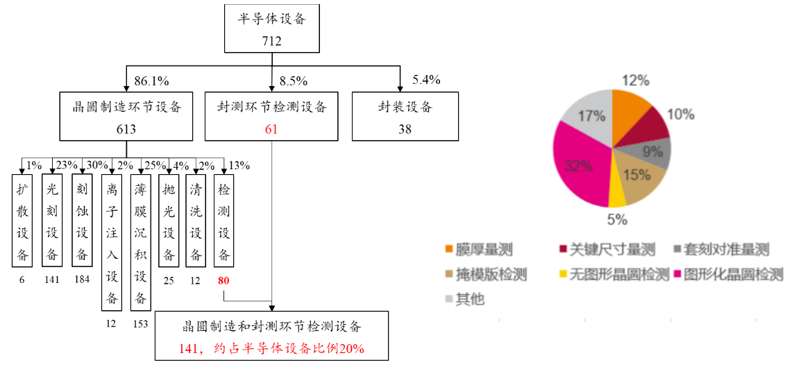
|In 2020, the global wafer manufacturing industry testing equipment market size will be about 8 billion US dollars In 2020, global semiconductor equipment sales were US$71.2 billion, a year-on-year increase of 19.2%, and China's semiconductor equipment sales were US$18.72 billion, a year-on-year increase of 39.2%. The proportion of semiconductor equipment sales in China increased from 14.5% in 2017 to 26.3% in 2020, becoming the largest market for semiconductor equipment for the first time. SEMI predicts that the global semiconductor equipment sales in 2021/2022 will be 95.3/101.3 billion US dollars. Assuming that the Chinese market share is stable at 26%, China's semiconductor equipment sales are expected to be 24.8/26.3 billion US dollars, or 160.4 billion yuan/170.1 billion yuan. +32%/+6% year-on-year respectively (RMB/USD exchange rate is 6.468, the same below). In 2020, wafer manufacturing accounted for 86.12% of semiconductor equipment sales. Semiconductor equipment mainly includes three types of wafer manufacturing equipment, (packaging and testing) testing equipment and packaging equipment. The SEMI report disclosed that the three accounted for 86.1%, 8.5% and 5.4% respectively in 2020. Wafer manufacturing mainly includes eight links, and the value of testing equipment in the wafer manufacturing link accounts for about 13%. In 2020, the sales of equipment in the wafer manufacturing process will be approximately US$61.3 billion, so it is estimated that the global market size of inspection equipment in the wafer manufacturing process will be US$7.969 billion in 2020. |Inspection equipment in wafer manufacturing is divided into measurement and defect detection, and the localization rate is extremely low Wafer manufacturing inspection equipment (process control) mainly includes measurement equipment and defect detection equipment, accounting for 40% and 50% of the value, respectively, and other equipment such as control software accounts for the remaining 10%. |Three classification standards: testing purpose, application scope, technical principle According to different classification methods, integrated circuits can be divided into different types. 1) According to the inspection purpose, it can be divided into measurement (Metrology) and defect inspection (DefectInspection) 2) According to the application category, it can be mainly divided into critical dimension measurement (OpticalCritical Dimension OCD), thin film thickness measurement (FilmMetrology), overlay alignment measurement (OverlayMetrology), reticle/mask inspection (ReticleInspection), patternless wafer inspection (Non-patternedWafer Inspection), Patterned Wafer Inspection (PatternedWafer Inspection), Defect Review (ReviewSEM) 3) According to the technical principle, it can be divided into optical inspection equipment (OpticalInspection Equipment), electron beam inspection equipment (E-beamInspection Equipment) and other inspection equipment. 1. Measurement of key dimensions The minimum line width in the semiconductor manufacturing process is generally called the critical dimension, and its variation is the key in the semiconductor manufacturing process. As the critical dimension gets smaller and smaller, the fault tolerance becomes smaller, so it is necessary to measure the line width of all products as much as possible. eg : Measure the line width and aperture of a circuit pattern at a specified location on a semiconductor wafer. 2. Film thickness measurement In the whole manufacturing process, there are many different types of thin films on the surface of the silicon wafer, including metals, insulators, polysilicon, silicon nitride and other materials. When a fab is producing chips with high reliability, the quality of the thin film becomes the key to improving the yield. The thickness, reflectivity, and density of the thin film all need to be accurately measured. eg: Measure the thickness of the thin film on the surface of the semiconductor wafer. 3. Overlay alignment measurement Overlay alignment measurement is applied after the photolithography process, and is mainly used to measure the alignment capability of the photolithography machine, reticle and silicon wafer. The metrology system inspects the overlay accuracy (overlay tool) measurement is used to inspect the shot overlay accuracy of the first and second layer patterns transferred onto the wafer. |Reticle/Mask Inspection: Capture reticle defects and pattern placement errors, reducing the risk of defect initiation Reticle/mask inspection is far more important than other applications such as unpatterned or patterned wafer inspection. This is because, while a single defect on a bare or patterned wafer has the potential to destroy one device, a single defect on a reticle can destroy thousands of devices. Usually, the mask is easy to absorb dust particles during use, and the larger dust particles are likely to directly affect the transfer quality of the mask pattern, which will further lead to a decrease in yield if not processed. Therefore, after exposure with a mask, the reticle is usually inspected with an integrated mask detection system, and if out-of-spec dust particles are found on the reticle, the wafers in the lithography process will all be reworked. The detection of mask defects in Fab is divided into two types: online and offline. In-line inspection refers to inspection of the mask surface before and after each exposure. The working principle of the mask inspection system can be seen in the figure below: this is usually done by relying on the built-in inspection unit in the lithography machine. Off-line inspection refers to periodically pulling the mask out of the system for defect inspection. |EUV reticle/mask inspection: shorter wavelength, higher detection sensitivity The traditional method of inspecting EUV photomasks is mainly to apply deep ultraviolet ( DUV ) light to the light source. Although DUV light can also be applied to the current most advanced process of 5 nanometers, Yutaro Misawa, director of the business planning office of Lasertec , pointed out, "With the development of miniaturization, when entering the 2 nanometer process, DUV 's photosensitive degree may not be sufficient” that is, the demand for inspection equipment using EUV light sources is expected to grow further. Extreme Ultraviolet (EUV) has a shorter wavelength than DUV and is more sensitive for product defect detection. The detection principle of EUV reticle is: electromagnetic waves are radiated to small defect particles and scattered to form a dark field, which can realize the detection of defects. The system uses a working wavelength of 364nm. For defects with a base size of 88nm, the detection feasibility is 97%. The demand for EUV mask (photomask, mask) inspection equipment for semiconductor circuits has grown particularly strong in recent years. In this field, Japan's Lasertec Corp. is the world's only testing machine manufacturer, holding 100% of the global market. share. |Unpatterned wafer inspection: Detect bare wafer particles and defects, laying the foundation for patterned inspection Unpatterned inspection refers to the inspection process in which bare wafers are certified at the wafer manufacturer before production begins, and re-certified inspections are received by semiconductor fabs. The rationale for defect inspection on patternless wafers is relatively simple. The laser beam is scanned radially across the rotating wafer surface to ensure that the beam hits all wafer surfaces. The laser light is reflected off the wafer surface, and when the laser beam encounters particles or other defects on the wafer surface, the defects scatter part of the laser light. Loss of intensity in scattered light (dark field illumination) or reflected beam (bright field illumination) can be directly detected, and particle/defect position coordinates are calculated and recorded from the wafer rotation angle and the radius position of the laser beam. The rotational position of the wafer and the radial position of the beam determine the location of defects on the wafer surface. In the wafer inspection tool, the light intensity is recorded using a PMT or CCD method and a map of the scattered or reflected intensity of the wafer surface is generated. This graph provides information on defect size and location, as well as information on wafer surface condition due to issues such as particle contamination. | Patterned wafer inspection: Compare images to generate defect maps to identify physical and high aspect ratio defects Patterning Definition: Patterning uses photolithography and optical masking to imprint patterns that guide the deposition or removal of material from the wafer surface at specific steps in the device fabrication process. For each layer of the device, material is deposited or removed in areas not covered by the mask, and a new mask is used to process the next layer. Wafers are repeatedly processed in this manner, thereby producing multi-layer circuits. Optical inspection of patterned wafers can use brightfield illumination, darkfield illumination, or a combination of both for defect detection. In addition, electron beam (EB) imaging is also used for defect detection, especially in smaller geometries where optical imaging is less effective. However, it is very slow and is only used in the R&D phase. Die wafer inspection systems compare an image of a test die on a wafer with an image of an adjacent die (or a known defect-free "gold" die). The location of the defect generates a defect map, similar to the map generated for unpatterned wafers. Like the inspection of unpatterned wafers, patterned wafer inspection requires precise and repeatable motion control, with the wafer level and optics of the test system moving simultaneously. |Defect review and inspection: zoom in on the defect image for identification, and provide the basis for optimizing the process technology With the advancement of semiconductor integrated circuit process nodes, the resolution of optical defect inspection equipment, which is the main equipment for fab process control, can no longer meet the needs of large-scale production and advanced process development, and must rely on higher-resolution electron beam re-inspection equipment. Only by further review can the defects be clearly imaged and typed, so as to provide a basis for semiconductor process engineers to optimize the process technology. Defect review is the use of scanning electron microscopy (SEM) to inspect wafers for defects. Use Defect Review to magnify defects detected by a semiconductor wafer defect inspection system into a high-magnification image for review and classification. Defect review equipment is primarily used with inspection systems for electronic equipment and other semiconductor production lines. |Technical principle classification: optical, electron beam detection, application complementary, multi-directional detection Optical inspection and electron beam inspection are complementary in the inspection of process technology. The characteristics of optics are fast and complete, and can usually be detected around the clock. In the application scenarios that require real-time detection and are close to the process machine or even directly integrated with the process machine, optical detection is used. The reflection and diffraction spectra of light are used for detection. Measurement has the advantages of fast detection speed, low cost and wide range; however, the wavelength of traditional optics is at the nanometer level, and very fine detection cannot be done, so electron beams will be used for finer detection. The electron beam wavelength is on the picometer scale, and images can be collected at high resolution for classification and analysis. The inspection of the process must be accurately evaluated. If the process deviation and potential yield problems are not detected, the produced products will be unusable. Therefore, multiple inspection equipment is required for multi-directional inspection. |KLA is the largest testing equipment in wafer manufacturing, with a market share of 58% in 2020 According to Gartner data, in 2020, KLA will account for 58% of the sales share of the wafer manufacturing inspection equipment market, while Applied Materials and Hitachi High-Tech will account for 12% and 5% respectively, and the three companies together account for 75%. The market concentration is high and It is monopolized by overseas companies. The main domestic companies include Shanghai Ruili, Jingce Electronics, Saiteng, etc., with a market share of less than 1%. |KLA: Leading Inspection Equipment in Wafer Manufacturing |Major Chinese Manufacturers: Grasp Market Segment Opportunities