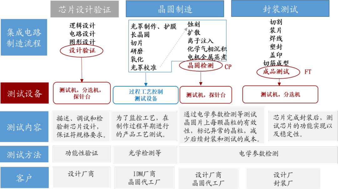
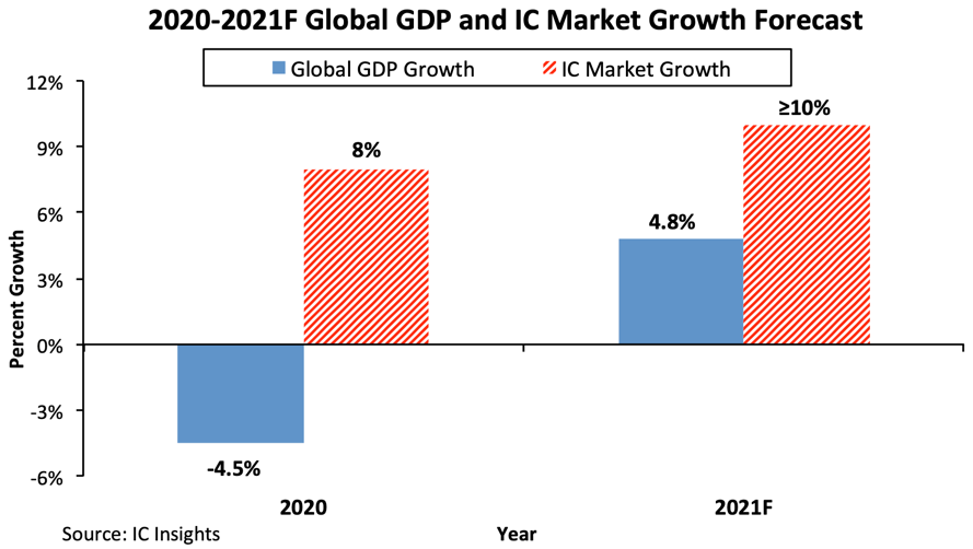
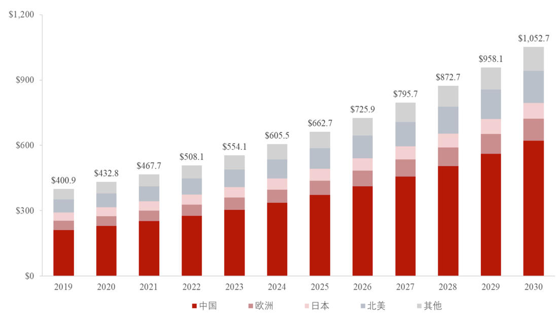
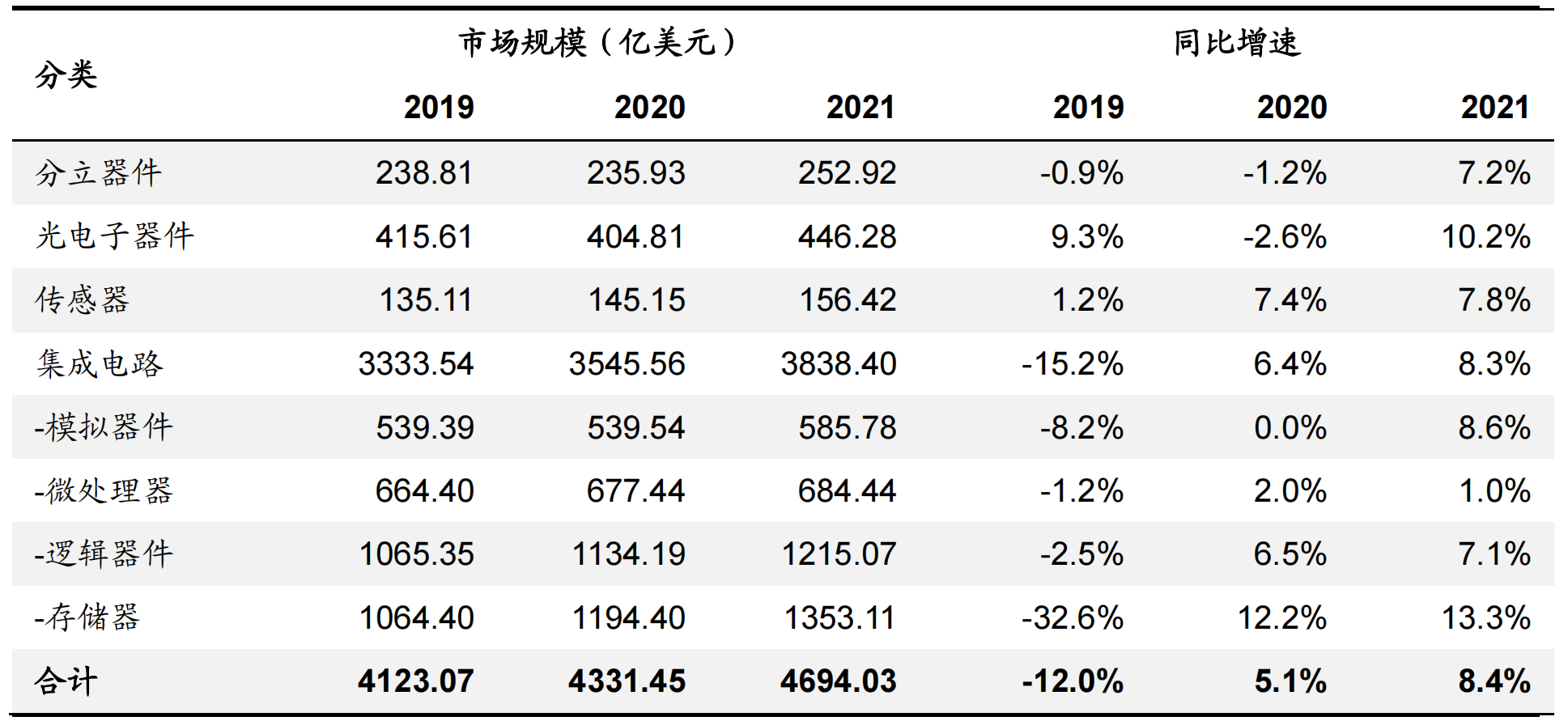
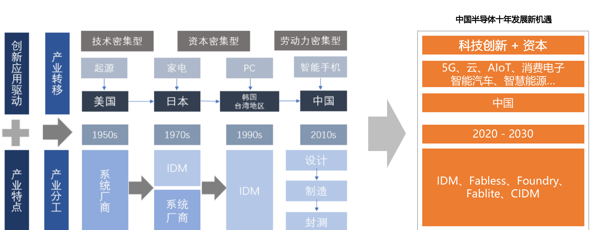
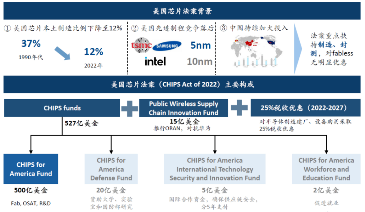
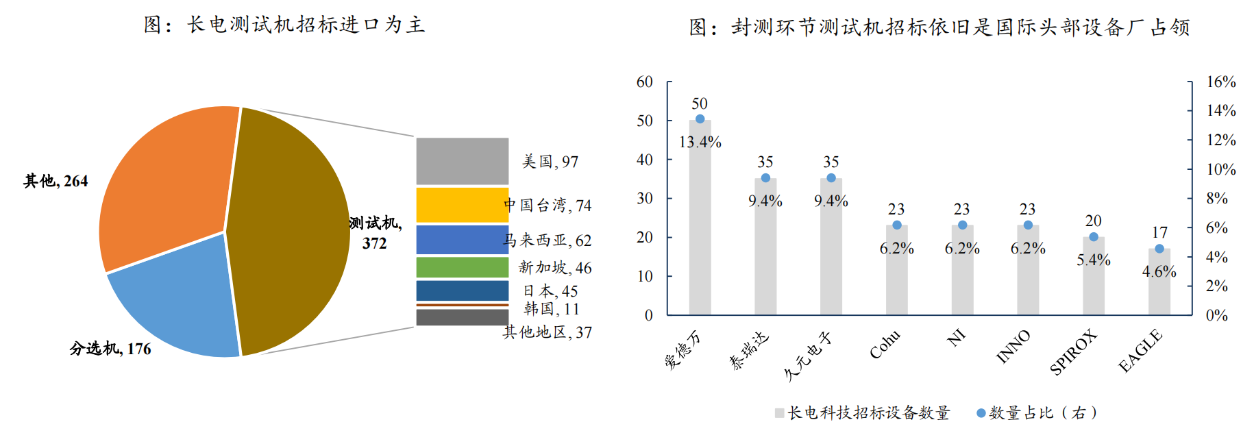
Market space: As the key to optimizing process control yield, improving efficiency and reducing costs, testing equipment occupies an important position in the semiconductor industry, accounting for about 20% of all semiconductor equipment, and the global market size is about 14 billion US dollars, of which the former 8 billion US dollars for road equipment, and 6.5 billion US dollars for downstream equipment. Among the world's top ten semiconductor equipment manufacturers, testing equipment manufacturers KLA, Teradyne, and Advan have three seats. Drivers: 1) Moore and Beyond Moore: Under the advanced semiconductor manufacturing process, the technology has doubled, and the detection accuracy requirements have increased exponentially; RF, MEMS, power supply and other Beyond Moore fields have become important growth drivers for the semiconductor industry and equipment with the development of automobiles and 5G. 2) Accelerating the migration of the semiconductor industry to China: Location advantages, international situations, and national policies jointly drive the accelerated migration of the semiconductor industry to China, bringing huge demand for equipment. 3) The US chip bill further stimulates domestic substitution: under the new chip bill, semiconductor equipment can have domestic substitution opportunities for at least ten years. Investment Opportunities: 1) The localization rate of front-end testing equipment is extremely low. At present, the leading domestic companies include Zhongke Flying Test, Shanghai Ruili, etc., which can widely pay attention to various early investment opportunities; 2) The localization rate of back-end testing equipment is relatively high, among which the testing machine focuses on SoC and storage testing machines; the probe station focuses on leading companies such as Shenzhen Silicon Power and Senmei Xieer; the sorting machine market structure is relatively scattered, and the future will be large. The probability is that listed companies such as Changchuan Technology occupy a dominant position. |Testing equipment: front-track quantity testing, back-track testing 1) Fore-channel quantity detection equipment (manufacturer): The front-end inspection object is the wafer in the process. It is a physical and functional test to detect whether the processing parameters of the product after each step of the process meet the design requirements, and to check whether the surface of the wafer is There are yield-impacting defects, ensuring that processing line yields are controlled above specified levels. The front-end inspection includes film thickness measurement equipment, OCD critical dimension measurement, CD-SEM critical dimension measurement, lithography calibration measurement, pattern defect inspection equipment and other front-end inspection equipment. Due to the complexity of the wafer manufacturing process, there are many types of testing equipment required, so it is also the link with the highest barriers in all semiconductor testing tracks. The suppliers of front-end testing equipment currently include Kelei and Applied Materials from the United States; Hitachi from Japan; and domestic precision testing electronics, Zhongke Flying Test, Shanghai Ruili and so on. Downstream customers are integrated circuit manufacturers, including TSMC, SMIC, YMTC, etc. 2) Back-end test equipment (designer and packaging and testing manufacturer): Applied in upstream design and downstream packaging and testing, the purpose is to check whether the performance of the chip meets the requirements. It is an electrical and functional test to check whether the chip meets the performance requirements. 1. Upstream designers need to verify the validity of the finished wafers and chip samples. The main equipment is testing machine, probe station, and sorting machine. Because they are used for sample testing, they usually do not purchase in large quantities, but they will cooperate with downstream equipment. Packaging and testing are deeply linked, so binding integrated circuit designers has also become one of the barriers for back-end test equipment manufacturers. The main downstream customers are integrated circuit designers, such as: Qualcomm, MediaTek, HiSilicon, Zhuoshengwei, Weir, etc. 2. The packaging and testing process can be mainly divided into: wafer testing (CP), which conducts electrical testing for the processed wafers to identify the chips that can work normally. The main equipment is the testing machine and the probe station. Some customers are integrated circuit manufacturers and some third-party wafer testers; finished product testing (FT), after the wafer is finally cut into chips, the final test is carried out for the performance of the chip, the main equipment is testing machine and sorting The downstream customers are integrated circuit packaging and testing companies, including ASE, Tongfu, Changdian, etc. The back-end test equipment suppliers currently include Teradyne and Advan from the United States; domestic precision testing electronics, Huafeng Measurement and Control, Changchuan Technology, etc. |The partial physical property is detected in the wafer manufacturing process, and the partial electrical performance is detected in the packaging and testing process |Moore's Law: Multiplication of Process Steps to Expand Market Space New application requirements have driven process scaling and 3D structure upgrades, which have greatly increased the number of process steps. The number of process steps for a mature process (take 45nm as an example) requires about 430, and the number of process steps for an advanced process (take 5nm as an example) will increase to 1250. , the process steps have been increased by nearly 3 times; structurally, the new generation of semiconductor processes including GAAFET, MRAM, etc. are becoming more and more complex. In thousands of processes, the detection of each process must not have errors, otherwise it will be significantly affected. The success or failure of the chip. |More than Moore: New applications emerge to drive market potential Analog/mixed-signal, RF, MEMS, image sensing, power and other technologies can be integrated with CMOS in various planes and even 2.5D, 3D architectures. These integrations and other key technologies enable the rapid growth of a range of applications such as artificial intelligence, IoT, and automotive radar. Yole Developpement data predicts that by 2023, the annual growth rate of the Beyond Moore market will total about 74 million silicon wafers in terms of wafer size, with a compound annual growth rate of about 3%. But considering only the most popular wafer sizes (12", 8", and 6" wafers), the forecast becomes 60 million wafers by 2023, a CAGR of about 5%. For semiconductor manufacturers , the More than Moore market has become a significant source of semiconductor demand, but this also means that new volume inspection and testing methods are required to accommodate the various failures that may affect these multi-technology devices. |Global semiconductor market: huge market size, rapid growth in the past three years The growth rate of integrated circuits in 2020 is 8%, far exceeding the growth of GDP. Similarly, the growth rate of integrated circuits is expected to be more than 10% in 2021, which is more than twice the growth rate of GDP. Handel Jones, CEO of IBS, an American electronics industry strategy consulting company, said at the SEMICONCHINA Forum in March 2021 that the global semiconductor market will reach US$1.1 trillion by 2030, and China's semiconductor market will account for 60% of the world's total |Global Semiconductor Market and Submarket Space and Growth According to the official website of the World Semiconductor Trade Statistics Organization (WSTS), the market size of the global semiconductor market in 2021 will be approximately US$469.4 billion, an increase of 8.4% year-on-year; It is expected to reach 8.6%, 7.1%, and 13.3% respectively. The market space of storage and logic devices exceeds 100 billion US dollars, which are the two largest markets in integrated circuits. |China: The third migration of the semiconductor industry is a major historical opportunity for China in the next decade The world has experienced three waves of industrial transfer. Among them, the first and second major industrial transfers have brought about the prosperity and development of the chip industry in Japan, South Korea, Taiwan, China and other countries and regions. There have also been rising stars such as Samsung and TSMC, which have become the leading companies in the global chip industry. . The semiconductor industry is accelerating its transfer to China. Facing emerging applications such as 5G, cloud, AI, and the Internet of Things, it gathers technological innovation and capital to rapidly improve the core capabilities of the industry. |China: U.S. chip bill drives major changes in the semiconductor industry The United States has introduced a bill for more than 50 billion chips, focusing on supporting semiconductor manufacturing and packaging and testing (high location costs lead to a lack of competitive advantage in US manufacturing packaging and testing), and the ban on the expansion of subsidized companies for 10 years, which means that the next 10 years Domestic substitution is still an unavoidable investment theme. Wafer fabs/packaging and testing plants: The expansion plans of international semiconductor giants in China have been terminated, and the production capacity of domestic wafers and packaging and testing plants is expected to continue to expand. At the same time, the global competition for cutting-edge technologies such as advanced manufacturing process and advanced packaging will continue to intensify. Equipment factories: On the one hand, they benefit from domestic substitution, and on the other hand, they also directly benefit from the continuous expansion of domestic wafer factories and packaging and testing factories. Design companies: Downstream end customers have to consider domestic chips as an alternative, providing a fairly long window for domestic design companies to enter the market. |The leader of testing equipment is firmly ranked among the top ten semiconductor equipment manufacturers in the world, with a solid business focus KLA, the leader in testing equipment in the wafer manufacturing process, and Advantech and Teradyne, the leader in testing equipment in the packaging and testing process, are among the top ten semiconductor equipment manufacturers in the world from 2017 to 2020, ranking 5th, 6th and 20th respectively. 8th. The global semiconductor equipment market is stable, with CR10 exceeding 76% in 2018-2020. In terms of specific ranking, the ranking of the 1st to 8th companies has not changed for three years (only the ranking of Fanlin Semiconductor and Tokyo Electronics will be exchanged in 2020, but the revenue scale of the two is not much different), and the 9th and 10th companies are in 2019. -2020 is also relatively stable. Different from other leading equipment manufacturers, the leading business of testing is more specific. The business of leading equipment companies such as Applied Materials, Lam, and Tokyo Electron covers multiple aspects of the semiconductor process, while KLA, Advan and Teradyne focus on testing equipment and involve less business in other aspects, and have absolute dominance in the main aspects. status. |Changdian core equipment bidding is basically 100% imported, and the process of localization has a long way to go In recent years, most of the testing machines, sorting machines and probe stations that have been publicly tendered for Changdian's core equipment are imported brands, mainly from the United States, Taiwan, Japan, Singapore and other countries and regions. Since the beginning of 2015, Changdian Technology has publicly tendered 372 testing machines, 176 sorting machines and 264 auxiliary equipment (probe stations, tape machines, etc.), which are rarely seen by mainland Chinese manufacturers. The bidding for testing machines is still occupied by international leading brands. Appearance inspection equipment in wafer manufacturing is mainly from KLA (US), MVP (US), and Teng Teng Technology (Taiwan, China), while the testing system/tester/tester in packaging and testing is mainly from Teradyne (US), Advantest (Japan) ), SPIROX (Taiwan, China), Cohu (United States), Jiuyuan Electronics (Taiwan, China) and other internationally renowned brands. The sorting machine is mainly supplied by Chinese Taiwanese and Korean manufacturers. The main suppliers are Hongjin Technology (Taiwan, China), HANMI (South Korea) and SEMES (South Korea), of which Hongjin Technology accounts for about 51% of the equipment. |The maturity of the domestic main industrial chain is a necessary condition for the development of domestic equipment manufacturers In the short term, the localization rate of semiconductor equipment will be improved, and the testing equipment in the packaging and testing process will be improved or faster. This is mainly due to the promotion of national policies (the first and second phases of large funds, etc.), the capacity expansion of wafer fabs and packaging and testing plants, the increase in domestic substitution demand and the technological catch-up of domestic equipment manufacturers against the background of chip shortage and Sino-US trade war. and shorten the verification period. Especially in the packaging and testing process, the three domestic international head packaging and testing factories have strong strength, with a combined market share of 20.9% in terms of revenue in 2020. The joint research and development of packaging and testing factories and testing equipment manufacturers in the packaging and testing process is more difficult or less, and this link is localized. Advances may be faster. In the long run, the maturity of the main domestic semiconductor industry chain is a necessary condition for the development of domestic equipment manufacturers. We judge that only when domestic fabs catch up with international leaders such as SMC, Samsung, and Hynix, and when domestic packaging and testing plants catch up with ASE, can equipment manufacturers usher in a historic turning point. Fab factories and packaging and testing factories need to overcome technical difficulties before considering cost reduction measures such as localization of equipment.
